2012年12月23日 星期日

Smart Response Technology - SRT


In computingSmart Response Technology (SRT) (pre-launch name SSD Caching) is a proprietary caching mechanism introduced in 2011 by Intel for their Z68 chipset (for theSandy Bridge–series processors), which allows a SATA solid-state drive (SSD) to function as cache for a (conventional, magnetic) hard disk drive.
SRT is managed by Intel Rapid Storage Technology software version 10.5 or later, and implemented in its device driver and the Z68 motherboard's firmware (option ROM). It is available only when the (integrated) disk controller is configured in RAID mode (but not AHCI or IDE modes) by implementing a style of RAID-0 striping. Write-back (Maximized mode) or write-through (Enhanced mode) caching strategy can be selected by the user. The maximum utilizable cache size on the SSD is 64 GB. Caching is done at the logical block addressing (LBA) level, not the file level.
Shortly before the announcement of the new chipset, Intel also introduced the Intel 311 (Larson Creek), a 20 GB single-level cell (SLC) solid-state drive, which it markets as suitable for caching. TRIM garbage collection is currently not supported for SRT caching devices, so the SSD's performance is solely maintained by its own firmware.

Maximized Mode vs Enhanced Mode
The tow different modes set up the SSD caching in different ways. Enhanced mode is designed for maximum security, reducing the possibility of data loss but also limiting write speed as it writes data to the SSD and HDD at the same time. Maximized mode is designed for optimum performance, writing data to the SSD and only periodically transferring it to the hard drive. This means that if anything should go wrong with the SSD, you could lose some data. The outcome of an SSD failure would depend largely on what the SSD was caching at the time of failure, so it's difficult to predict how it would affect your system.

資料來源: http://en.wikipedia.org/wiki/Smart_Response_Technology
http://www.hardwaresecrets.com/printpage/Intel-Smart-Response-Technology-Explained/1292

2012年12月22日 星期六

Intel CPU Roadmap


Intel processor roadmap


資料來源: http://en.wikipedia.org/wiki/Haswell_(microarchitecture)

Intel Haswell


The new chips will still be running on the same 22nm production process, but with a new architecture that should see the graphics performance of the HD 4600 graphics components doubling.
That should give us some rather tasty-performing Ultrabooks, and with the upgraded GT3E version of the HD graphics on the mobile side we should get some svelte gaming laptops too.
One of the interesting points is the increase in TDP from the 77W of the Ivy Bridge up to 84W in the new Haswell chips. I expect that’s mostly down to the beefier graphics components with higher clockspeeds.
Sadly there’s no boost in the general clockspeed of the CPUs themselves. We’re still limited to 3.5GHz for the top-end i7-4770K and 3.4GHz for the i5-4670K.
It’s not a surprise to see Intel isn’t upping the core count either – sticking to four cores/eight threads for the i7 series and four cores/four threads for the i5.

Performance

Compared to Ivy Bridge (expected):
  • At least 10% CPU performance increase.
  • Double the performance of the integrated GPU.

Features carried over from Ivy Bridge

  • 22 nm manufacturing process.
  • 3D tri-gate transistors.
  • A 14-stage pipeline (since the Core microarchitecture).
  • Mainstream up to quad-core.
  • Native support for dual channel DDR3.
  • 64 kB (32 kB Instruction + 32 kB Data) L1 cache and 256 kB L2 cache per core.

Confirmed new features

Haswell New Instructions (includes Advanced Vector Extensions 2 (AVX2), gather, bit manipulation, and FMA3 support).

Expected features

  • Shrink PCH from 65 nm to 32 nm.
  • A new cache design.
  • Up to 32MB Unified cache LLC (Last Level Cache).
  • Support for Thunderbolt technology.
  • There will be three versions of the integrated GPU: GT1, GT2, and GT3. According to vr-zone, the fastest version (GT3) will have 20 execution units (EU). Another source, SemiAccurate, however says that the GT3 will have 40 EUs with an accompanying 64MB cache on an interposer. An additional source, AnandTech, agrees that GT3 will have 40 EUs, and states there will be a version with up to 128MB of embedded DRAM, but makes no mention of an interposer.[27][28] Haswell's predecessor, Ivy Bridge, has a maximum of 16 EUs.
  • New advanced power-saving system.
  • Fully integrated voltage regulator, thereby moving a component from the motherboard onto the CPU.
  • 37, 47, 57W thermal design power (TDP) mobile processors.
  • 35, 45, 65, 84, and ~100W+ (high-end, Haswell-E) TDP desktop processors.
  • 10W TDP processors for the Ultrabook platform (multi-chip package like Westmere) leading to reduced heat which results in thinner as well as lighter Ultrabooks, but performance level will be lower than the 17W version.

Haswell Lineup

Haswell Lineup

資料來源: http://www.pcgamer.com/2012/12/13/intels-haswell-i5-and-i7-line-ups-leaked/
http://en.wikipedia.org/wiki/Haswell_(microarchitecture)

Intel Management Engine Interface - IMEI


IMEI is one component of Intel's VPRO remote access technology.

From what I can understand of the technical literature it is to allow remote access over a LAN for IT admin / repair purposes even when the system is powered down.


The Intel Management Engine (Intel ME) refers to the hardware features that operate at the baseboard level, below the operating system. By enabling interaction with low-level hardware, Intel gives administrators the ability to perform tasks that previously required someone to be physically present at the desktop.
The initial setup of Intel's Management Engine starts by activating it in a compatible PC’s BIOS. Once you enable Intel's ME, you gain access to several BIOS functions.
You're required to configure an initial administrative password the first time you enter the ME BIOS interface.
As you can see in the screen shot above, Intel's Active Management Technology (AMT) is turned on through the management engine.
Generally, you want to enable the option "ON in S0, ME Wake in S3, S4-5". This translates to the management engine and AMT being on when the host is powered up. When the host is in S3 to S5 and the platform is connected to AC power, the management engine shuts down after a defined period of time, but wakes back up when it receives a network message. By using this feature, an IT department can allow desktops to sleep, saving power, and then wake up once everyone goes home and the admin can push out updates using cheaper energy.
Within these same BIOS screens, you can perform several different low-level AMT-related configuration tasks.
Intel lets you save certificates for a given environment to the management engine so that a PC can authenticate prior to being granted network access.

WOL vs ME
Classic WOL has inherent weaknesses for DOS attacks - ME WOL requries authenticated users to wake the system and can even include CA's and Cerberus encryption coverage. The cool thing is you can shut a system down remotely and have ME WOL avaialbe to wake the system up any time and any where, securely - we have a number of success stories about Me WOL and how much power is being saved, check it out
資料來源: http://www.tomshardware.com/reviews/vpro-amt-management-kvm,3003-6.html
http://communities.intel.com/thread/3165

2012年12月21日 星期五

Intel Active Management Technology - AMT

Intel Active Management Technology (AMT) is hardware-based technology for remotely managing and securing PCs out-of-band. Currently, Intel AMT is available in desktop PCs with Intel Core 2 processor with Intel vPro technology and available in laptop PCs with Centrino or Centrino 2 platform with vPro technology.

Intel AMT is hardware and firmware technology that builds certain functionality into business PCs in order to monitor, maintain, update, upgrade, and repair PCs. Intel AMT is part of the Intel Management Engine, which is built into PCs with Intel vPro technology. Intel AMT is designed into a secondary (service) processor located on the motherboard.

AMT is not intended to be used by itself; it is intended to be used with a software management application.[1] It gives a management application (and thus, the system administrator who uses it) better access to the PC down the wire, in order to remotely and securely do tasks that are difficult or sometimes impossible when working on a PC that does not have remote functionalities built into it


Hardware-based management and software-based management

Hardware-based (or out-of-band) management is different from software-based (or in-band) management and software management agents. Hardware-based management works at a different level than software applications, uses a communication channel (through the TCP/IP stack) that is different from software-based communication (which is through the software stack in the operating system). Hardware-based management does not depend on the presence of an OS or locally installed management agent.

DHCP, BOOTP, WOL vs Intel AMT hardware-based management

Hardware-based management has been available on Intel/AMD based computers in the past, but it has largely been limited to auto-configuration using DHCP or BOOTP for dynamic IP allocation and diskless workstations, as well as Wake-on-LAN (WOL) for remotely powering on systems

Intel AMT features


Intel AMT includes hardware-based remote management, security, power-management, and remote-configuration features. These features allow an IT technician to access an AMT featured PC remotely.
Intel AMT relies on a hardware-based out-of-band (OOB) communication channel that operates below the OS level, the channel is independent of the state of the OS (present, missing, corrupted, down). The communication channel is also independent of the PC's power state, the presence of a management agent, and the state of many hardware components (such as hard disk drives and memory).
Most AMT features are available OOB, regardless of PC power state. Other features require the PC to be powered up (such as console redirection via serial over LAN (SOL), agent presence checking, and network traffic filtering).[1] Intel AMT has remote power-up capability.
Hardware-based features can be combined with scripting to automate maintenance and service.

Hardware-based AMT features in laptop and desktop PCs

Hardware-based AMT features include:
  • Encrypted, remote communication channel for network traffic between the IT console and Intel AMT.
  • Ability for a wired PC (physically connected to the network) outside the company's firewall on an open LAN to establish a secure communication tunnel (via AMT) back to the IT console. Examples of an open LAN include a wired laptop at home or at an SMB site that does not have a proxy server.
  • Remote power up / power down / power cycle through encrypted WOL.
  • Remote boot, via integrated device electronics redirect (IDE-R).
  • Console redirection, via serial over LAN (SOL).
  • Keyboard, video, mouse (KVM) over network.
  • Hardware-based filters for monitoring packet headers in inbound and outbound network traffic for known threats (based on programmable timers), and for monitoring known / unknown threats based on time-based heuristics. Laptops and desktop PCs have filters to monitor packet headers. Desktop PCs have packet-header filters and time-based filters.
  • Isolation circuitry (previously and unofficially called "circuit breaker" by Intel) to port-block, rate-limit, or fully isolate a PC that might be compromised or infected.
  • Agent presence checking, via hardware-based, policy-based programmable timers. A "miss" generates an event; you can specify that the event generate an alert.
  • OOB alerting.
  • Persistent event log, stored in protected memory (not on the hard drive).
  • Access (preboot) the PC's universal unique identifier (UUID).
  • Access (preboot) hardware asset information, such as a component's manufacturer and model, which is updated every time the system goes through power-on self-test(POST).
  • Access (preboot) to third-party data store (TPDS), a protected memory area that software vendors can use, in which to version information, .DAT files, and other information.
  • Remote configuration options, including certificate-based zero-touch remote configuration, USB key configuration (light-touch), and manual configuration.
  • Protected Audio/Video Pathway for playback protection of DRM-protected media.

Intel® Active Management Technology Overview (pdf file)


Intel AMT Release 2.0 is a component of the Intel® vPro workstation platform. It uses a number
of elements in the Intel vPro platform architecture. Figure 1 shows the relationship between these
elements.


The Intel AMT functionality is contained in the firmware (ME FW).
• The firmware image is stored in the Flash memory.
• The Intel AMT capability is enabled using the Intel® Management Engine (Intel® ME) BIOS extension as implemented by an OEM platform provider. A remote application performs enterprise setup and configuration.
• On power-up, the firmware image is copied into the Double Data Rate (DDR) random-access memory (RAM).
• The firmware executes on the Intel ME processor and uses a small portion of the DDR RAM (Slot 0) for storage during execution. RAM slot 0 must be populated and powered on for the firmware to run.


Intel AMT stores the following information in the Flash (ME Data):
• OEM-configurable parameters 
• Setup and configuration parameters such as passwords, network configuration, certificates, 
and access control lists (ACLs) 
• Other configuration information, such as lists of alerts and System Defense policies 
• The hardware configuration captured by the BIOS at startup 

Intel AMT Release 2.5 Architecture 
Intel AMT Release 2.5 extends active management to enterprise wireless mobile computing. As
shown in Figure 2 below, the architecture has a mobile version of ICH8, the Crestline MCH and a
wireless NIC.


資料來源: http://en.wikipedia.org/wiki/Intel_Active_Management_Technology
http://software.intel.com/sites/default/files/m/2/3/8/9/c/17992-intel_amt_overview.pdf

2012年12月18日 星期二

Intel S-Spec number

What is an sSpec?
The sSpec number is also known as the specification number and SL or SR code. It is a five character string (SL36W, SR00B, etc.) that is printed on the processor topside and is used to identify the processor. They usually start with the SL or SR and are followed by three alphanumeric characters.

Do all processor numbers have the same sSpec?The same processor number can have different sSpecs. The reason is because when a processor stepping change occurs, a new sSpec is generated for that stepping. It is also true that the same stepping level can also have more than one sSpec associated with it.

What is a stepping?
In its simplest form, it is a revision of the processor silicon. These are divided into two types. One type is called a full-layer stepping in which all the masks used to create the silicon can change. The other type is called a metal-layer stepping in which only the masks which are regenerated are the metal layers, allowing for fewer possible changes.

When steppings change, what is the naming convention?Each stepping gets a different name. The usual naming convention is to change the letter of a stepping on each full-layer stepping and change the number of a stepping on the metal-layer stepping. As an example, the first full-layer stepping from A0 would typically be B0 and the first metal-layer stepping from A0 would be A1.


Where can I find more information about my processor based on the sSpec or processor number information?For processor specifications and comparisons, Intel recommends visiting theirproduct information web site. You can use the search box in the upper right hand corner to find your processor specifications. Some of the searchable terms include sSpec, processor number, processor codename, product order code, or brand name. You also have the option of using the menu to drill down on the information for the processor you are looking for.
You can also find out more information in the processor family technical documents page under the datasheet section and specification update section. To see an example, go to Intel® Core™ i7 Technical Documents.


The sSpec number, also known as the specification number and SL code, is a five character string (SL36W or XL2XL, for example) printed on the processor or processor label.
How to find the sSpec number:
  • Read the boxed processor label as shown in Figure 1 below, or
  • Look at the markings on the processor as shown in Figure 2 below.
Figure 1: Find the sSpec number on the boxed processor label:
Figure 2: Find the sSpec number in the processor markings (two examples)


資料來源: http://www.intel.com/support/processors/sb/cs-016552.htm
http://www.intel.com/support/processors/sb/CS-028738.htm

2012年12月17日 星期一

ES vs QS CPU

一般CPU正式出來之前會有兩個版本...
ES跟QS;
ES是從Unit Test開始,通常這種CPU很多都是第一批,穩的很穩,有問題的就很@*&)#....
因為要經過很多長時間的測試,所以體質有可能比較好些,
不過...買到好的還是不好的就要看運氣或者是看跟誰買哩...

QS通常都是後面的Stage,已經要出貨或者接近出貨的了,
由CPU廠商提供比較近似於到時候市場可以買的到的了..

不過這部份我想不管是es或者qs應該都是後端流出來的,應該是沒有保固的唷!
但相對的價格應該會比正式版的便宜些的!

QS是Quantity Sample(應該是這樣拼吧?)
是ES版的後續
算是出貨前最後一個測試版
不過還是一樣 是工程樣品
非正式販售的版本

其實ES也是有分A1 B1的

Pre-ES1 < ES1 < ES2 < Pre-QS < QS < GS < formal release


鐵蓋上面一樣會有QS的序號 Qxxx
QJBP <--這個值叫做QDF,是Intel ES版CPU專用的代號格式
只會代表唯一Intel的某一顆CPU


Pentium® (C-1) Processor Mark Diagram The next several pages show the mark diagrams for:
  • Production units of the the new Pentium® Processor C-1 Stepping with heatspreader (the inner box-outline in the diagram below)
  • Samples of the C-1 Stepping (again with the heatspreader)
  • Production mark diagram for the B-1'' stepping without the heatspreader for comparison.
Production Mark Diagram
Notes:
The inner line box defines the edge of the heatspreader.
Ink Mark = All Logo information on the heatspreader.
Laser Mark = The two lines of information above and below the heatspreader.
SS = Speed
NNN = Specification Number
FFFFFFFF = FPO # (Test Lot Traceability #).


Pentium® (C-1) Processor Mark Diagram Samples Mark Diagram
The mark diagram for samples is identical to production units with one exception:
    The second line of the sample mark diagram begins with 'Q' instead of 'S'. The rest of this line is a QDF # instead of an S-spec #; samples are ordered by QDF#.
Notes:
The inner line box defines the edge of the heatspreader.
Ink Mark = All Logo information on the heatspreader.
Laser Mark = The two lines of information above and below the heatspreader.
SS = Speed
NNNN = Sample QDF number
FFFFFFFF = FPO # (Test Lot Traceability #).


資料來源: http://www.coolaler.com/showthread.php/262697-%E8%AB%8B%E5%95%8F%E4%BB%80%E9%BA%BC%E6%98%AF%E3%80%90Pre-QS%E3%80%91%E7%9A%84%E7%94%A2%E5%93%81%EF%BC%9F
http://www.mobile01.com/topicdetail.php?f=296&t=2112122
http://www.coolaler.com/archive/index.php/t-165496.html
http://www.intel.com/support/processors/pentium/sb/cs-011042.htm


2012年12月16日 星期日

UEFI - Unified Extensible Firmware Interface


凡依照UEFI論壇規範,使用C語言寫作的BIOS即為UEFI BIOS

EFI Shell常用指令
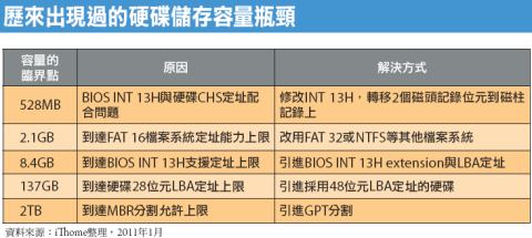
傳統MBR格式的磁碟分割,是透過32位元來描述磁碟的起始點和大小,最高只支援2.2TB的磁碟容量(512bytes x 2 ^ 32磁區)和4個主要分割區。
UEFI支援的GPT磁碟分割,使用64位元數值來描述分割區,最高支援1680TB的磁碟大小及100個主要分割區。512Bytes x 2^64 = 2^3 x 2^70

傳統BIOS開機流程


1. 初始化:

當電腦打開,CPU會自行重置為初始狀態,準備運作。BIOS boot block(基本輸出輸入系統開機區塊)初始化階段啟動,因為此時系統記憶體中是空的,沒有內容可以執行,所以廠商讓CPU去尋找系統BIOS ROM中的reset vector(重置向量):用一個固定的位置來啟動所謂的BIOS boot program開機程式。
一般來說程式會在記憶體的FFFF0h位址,也就是在UMA(上層記憶區域)靠結尾的地方。為避免ROM大小改變造成相容性的問題,所以一般會選擇放這裡。它的內容只有一個jump指令,進一步跳到真正的BIOS啟動程序。當然了,各家IBV independent BIOS vender;獨立BIOS供應商)可以把程式放在不同的位置,只要透過jump來指定就可以了。
在這段期間,系統的CPU、晶片組、Super I/OUSB只有部分初始化,僅獲取足夠資料來應付萬一BIOS開機失敗,可以利用軟碟(由Super I/O控管)甚至是光碟(由晶片組的IDE/SATA)等儲存媒體來救援BIOSboot block

2. POSTPower On Self Test;開機自我檢測):

然後BIOS開始施行Power-On Self TestPOST;開機自我檢測),在過程中檢查電腦各項組件及其設定,像是:中央處理器、主記憶體、鍵盤、滑鼠等等狀態。接著便尋找被內建在BIOS內部的顯示卡程序並執行。
它通常被放在記憶體C0000h的位置,作用是顯示卡的初始化,而大部分的顯示卡都會在顯示器上顯示其相關訊息。這就是為何各位在開機的時候,首先會在顯示器的畫面左上角出現有關顯示卡訊息的原因。
再下來就是讓BIOS尋找其他裝置的ROM(唯讀記憶體),看看這些設備中哪些還有個別的BIOS。如果這時有找到任何其它裝置的BIOS,它們也會被執行。
下一步BIOS會顯示啟動畫面,並開始更深入的檢測,包含我們平常可以在螢幕上看到的記憶體容量檢測。如果這時候遇到任何錯誤,就會在畫面上顯示錯誤訊息。

3. 記錄電腦系統的設定值:

到這裡還沒有結束,再來BIOS會根據自己的「系統資源表」,來對系統進行進一步的確認,看看你的電腦究竟安裝了那些系統資源或設備。有些電腦會逐步顯示這些被偵測到的設備。例如BIOS支援隨插即用,那它將會偵測和配置隨插即用裝置,並顯示由BIOS偵測到的隨插即用設備。
在這些檢測結束後,BIOS會打出一個偵測總結表於畫面上。而這個總結表在部分IBV的設定中是可以讓使用者開啟或關閉的。當然也有些IBV為加速開機把這一步直接隱藏省略。
Tips:BIOS boot block
在快閃唯讀記憶體內,通常會分成兩個區塊,一個區塊存放一般的BIOS程式碼,即所謂的code block(程式碼區塊);另一個區塊則是存放用來開機(或急救)的程式碼,就是所謂的boot block(開機區塊)。當電源打開時,主機板會先從boot block執行,它會立即檢查code block 的程式碼是否正確,如果正確,就會轉到code block 繼續執行下去。而所謂的BIOS recoveryBIOS回復)就是利用boot block回寫動作來進行BIOS更新失敗時的救援。

4. 提供常駐程式:

提供作業系統或應用程式呼叫的中斷向量,如INT 10hVGA圖形及文字輸出中斷)等。

5. 載入作業系統:

到這裡是系統檢測的部分,接下來BIOS便開始尋找開機裝置,使用者可以透過在BIOS的設定來決定搜尋順序,目前常見的開機設備至少包含FDDHDD以及光碟機和USB開機裝置等多項。
找到開機裝置後,BIOS將會搜尋開機訊息以進行作業系統的開機過程。如果是找到了一個灌好OS的硬碟,它將會尋找位在硬碟第0面,第0軌,第1磁區裡的Master Boot Record(主要開機磁區)。如果它找到的是FDD,也會讀取軟碟的第1磁區。再把讀取到的資料放在記憶體7C00h的位置,跳到那裡並且執行它。自此才開始進入OS啟動階段。

UEFI BIOS系統的開機流程


1. SEC階段:

SEC(安全性)階段其主要的特色為「cache as RAM」,即處理器的快取當成記憶體。由於C語言需要使用堆疊,在這個階段的系統記憶體尚未被初始化,在沒有記憶體可用的情況下,便把處理器的快取當成記憶體來使用,在主記憶體被初始化之前來進行預先驗證CPU/晶片組及主機板。
因為這時侯沒有快取,會導致處理器的效能變得較差,所以在記憶體初始化完畢之前,SECPEI階段的程式碼越簡短,越能減少這個副作用。

2. PEI階段:

和傳統BIOS的初始化階段類似,PEIEFI前初始化)階段是用以喚醒CPU及記憶體初始化。這時候只起始了一小部分的記憶體。同時,晶片組和主機板也開始初始化。接下來的服務程式會確定CPU晶片組被正確的初始化,在此時,EFI驅動程式派送器將載入EFI驅動程式記憶體,進入了起始所有記憶體的DXE階段(驅動程式執行環境)。

3. DXE階段:

DXE的主要功能在於溝通EFI驅動程式及硬體。也就是說此階段所有的記憶體、CPU(在此是指實體兩個或以上的非核心數目,也就是雙CPU插槽處理器甚至是四CPU插槽處理器)、PCIUSBSATAShell都會被初始化。

4. BDS階段:

BDS(開機設備選擇)這個階段,使用者就可以自開機管理者程式頁面,選擇要從哪個偵測到的開機設備來啟動。

5. TSL階段:

然後進入TSL(短暫系統載入)階段,由作業系統接手開機。除此之外,也可以在BDS階段選擇UEFI Shell,讓系統進入簡單的命令列,進行基本診斷和維護。

傳統BIOS哪裡不好?


1. 過時的16位元模式

x86系列CPU進入32位元的時代,為了相容性考量,當時最新的80386 CPU保留了16位元的執行方式,即真實模式(real mode)。在後來多次的CPU改朝換代中都保留了這種執行方式,甚至在含有EM64TXeon系列CPU中,供電到CPU啟動時仍然會切換到16位元的真實模式下執行。
也就是說,雖然各大BIOS廠商為了配合潮流演進,將許多新功能新元素添加到產品中,但BIOS在本質上沒有任何改變。迫使Intel在開發更新的CPU時,都必須加進會使效能大大降低的相容模式。


2. 只有1MB定址空間

各位讀者如果有注意傳統BIOS開機,在POST完畢後螢幕上打出的系統摘要表,會發現記憶體欄位標示著「Base Memory=640KB」。加上前一篇提到的384KB UMA(這裡的記憶體不會列入Base Memory),就是所謂1MB可定址記憶體空間


會造成這項限制,主要還是真實模式的副作用。16位元的CPU其定址能力為20條定址線所能處理的2^20位元組(Bytes),也就是1024千位元組(KB換句話說,在進入OS之前的開機階段,即使安裝了高達4GB的記憶體,絕大部分都無法使用。
2^20 Byte = 2^10 x 2^10 = 1 MB
IBM推出的第一台PC机采用的CPU8088晶元,它只有20根地址线,也就是说,它的地址空间是1MB PC机的设计师将1MB中的低端640KB用作RAM,供DOS及应用程式使用,高端的384KB则保留给ROM、视频适配卡等系统使用。从此,这个界限便被确定了下来并且沿用至今。低端的640KB就被称为常规记忆体即PC机的基本RAM区。
1985年初,LotusIntelMicrosoft三家共同定义了LIMEMS(Expanded Memory Spec,即扩充记忆体规范,通常称EMS为扩充记忆体。
我们把1MB以上的地址空间称为扩展记忆体XMSeXtend memory 386以上档次的微机中,有两种存储器工作方式,一种称为实地址方式或实方式,另一种称为保护方式。在实方式下,物理地址仍使用20位,所以最大定址空间为1MB,以便与8086相容。保护方式采用32位物理地址,定址范围可达4GB OS系统在实方式下工作,它管理的记忆体空间仍为1MB,因此它不能直接使用扩展存储器。为此,LotusIntelASTMicrosoft公司建立了MSDOS下扩展记忆体的使用标准,即扩展记忆体规范XMS。我们常在Config.sys文件中看到的Himem.sys就是管理扩展记忆体的驱动程式。
1MB以上空间的第一个64KB。我们把它称为高端记忆体区HMAHigh Memory Area)。HMA的物理存储器是由扩展存储器取得的。因此要使用HMA,必须要有物理的扩展存储器存在。
UMBUpper Memory Blocks)称为上位记忆体或上位记忆体块。它是由挤占保留记忆体中剩馀未用的空间而产生的,它的物理存储器仍然取自物理的扩展存储器,它的管理驱动程式是EMS驱动程式。

3. 組合語言難維護

假設某天你買了一張高階工作站主機板,再裝上一張SCSISAS的磁碟陣列卡,竟然發現安裝後你的主機板開機開不下去,然後顯示「Not enough space to copy PCI option ROM」或「Option ROM memory space exhausted」警告字串。然後本來你那雀躍快樂的心情消失了,取而代之的是「歸LP火」熊熊燃燒著。
當你打電話給陣列卡商,電話那頭的死公務員聲音說著:「你要不要問問主機板廠有沒有新的BIOS?」。 好不容易找上主機板廠商客服問:「你們有沒有辦法解決?」然後,你和主機板BIOS工程師之間的攻防就此展開。
對板卡廠的BIOS工程師而言,除非剛好有下單下很大的客戶遇到類似相關問題,否則很有可能就是不了了之。你只好趁購買七天內退掉那張陣列卡,不然就是再找一張可以正常搭配的主機板。
由於傳統BIOS是用組合語言編寫的,而軟體界早就已經是C/C++高階語言甚至是.NET滿天飛,為了相對難找的人才(組合語言高手相對少,要BIOS真正寫得好的更是少數)來減緩新產品上市的速度,不管是消費者或廠商都無法接受。
此時UEFI BIOS標準化和模組化的特徵,便可加速產品推出和減少debug的時間。另外C語言寫的UEFI BIOS體積也會變大,連帶使儲存BIOSEEPROM需要擴增。
別忘了,這也是Intel的勢力範圍,如果EFI BIOS推廣成功,板卡廠就得多採購一顆晶片。

4. 十年不變的程式碼

上述三大問題是以開發廠商的角度來觀察。其他隱而不現的部分,則包含了功能的侷限性和對使用者不夠友善的操作介面。對照現今的視窗介面作業系統,傳統BIOS以文字介面為主且充滿著火星文,加上除了單純的開機,作為仲介硬體初始化和作業系統的功能外實在陽春的可憐。
在開發Itanium CPU之際,業界大魔王Intel實在不想再受制於這些顧慮。試想,既然這是一個新生的CPU架構,那系統韌體和作業系統之間的介面就順便一起重新定義。
並且這一次,Intel為了讓以後各種新的規格和技術可以快速導入,嚴格定義這個傳統BIOS接班人必須具有擴展彈性,而且採取標準化的韌體介面規範,以避免發生傳統BIOSIBV程式碼更新太被動的問題。

UEFI BIOS哪裡好?


1. 定址空間更彈性

UEFI BIOS利用載入EFI driver的形式,來進行硬體的辨識/控制及系統資源掌控。
傳統BIOS是以真實模式中斷向量的方式增加硬體功能。它要將一段類似於驅動程式的16位元代碼,放置在記憶體0x000C00000x000DFFFF之間。這段記憶體空間有限(128KB),因此,當必須放置的option ROM超過128KB時,傳統BIOS便無能為力。
DFFFF-C0000=1FFFF=2 x 2^16=2^7 x 2^10=128KB
很多時候傳統BIOS的工程師為了解決這類問題,像剛剛提到的介面卡BIOS容量過大,便要想辦法利用可能的排列組合硬擠出空間來放驅動代碼。而重組過程有時不小心造成一些副作用,例如才剛解決的bug,重組後又再發生!也就是說,UEFI BIOS可以更有系統的分配儲存空間,避免使用強制定址。

2. 什麼系統都能用

另外,傳統BIOS的硬體服務程式都是以16位元代碼的形式存在,在增強模式下執行的作業系統想存取這些服務會有困難。因此BIOS提供的服務在現實中只能提供給MS-DOS之類的系統用。
相對的,UEFI系統下的驅動並不是可以直接在CPU執行的代碼,而是用EBCEFI Byte Code)這種專用於EFI driver的虛擬機器指令,該指令必須在UEFIDXE階段被解壓縮後翻譯執行。
如此便有更佳的向下相容性,因為EFI driver是彈性的驅動程式模組架構,可不斷的擴充驅動程式及介面,不用重新編寫,所以就無需考慮因系統升級所衍生的相容性因素。

3. 開發維護更容易

加上EFI driver開發簡單,所有的PC零組件廠商都可以參與,就像現代作業系統的開發模式,這樣的模式曾使Windows系統短短幾年就變得無比強大。有了EFI driver,也可以讓顯示卡在開機階段就載入某種程度的功能,進而可以把傳統文字介面為主的BIOS轉成圖形介面。

4. 精簡系統用途大

最後還有EFI Shell,這是個精簡的作業系統,可以讓使用者進行BIOS的更新、系統診斷、安裝特定軟體。有了UEFI BIOS甚至可以播放CDDVD而不需完全載入OSEFI driver可以被載入或卸載,連TCP/IP核心程式都可以使用。基於EFIdriver model可使UEFI系統接觸到所有的硬體功能,在進入作業系統之前瀏覽網站不再是天方夜譚,甚至實作起來也非常簡單。總之,對使用者而言,多了一個方便的環境以及華麗的圖形介面,是最明顯的好處。


UEFI由以下幾個部分所組成:
1Pre-EFI初始化模組
2EFI驅動執行環境(DXE)
3EFI驅動程式
4.兼容性支援模組(CSM)
5EFI高層應用 
6GUID磁碟分割表(GPT)
解決MBR分割所帶來的2TB限制問題。理論上可支援高達9.4ZB的磁碟分割區


我的網誌清單